• Log In
  • Home
  • About
    • People
    • Advisory Board
    • Staff Expertise
    • SENIC Research Impact
    • Success Stories and Testimonials
    • User Interviews
  • Facilities and Tools
    • SENIC Tools
    • Rates
    • Technical Webinars
    • SENIC Catalyst Program
    • Acknowledgements
    • Southeastern Nano Facility Network
  • Education and Outreach
    • Workshops
    • Summer Internships
    • Research Experience for Teachers
    • Seminars
    • Schedule a Visit
    • Education Resources
  • Society and Ethics
    • SENIC Ethics Video
    • NSF I-Corps
  • NNCI
  • News and Events
    • Newsletter
    • Photos
  • Contact Us

SENIC

Southeastern Nanotechnology Infrastructure Corridor

Southeastern Nano Facility Network

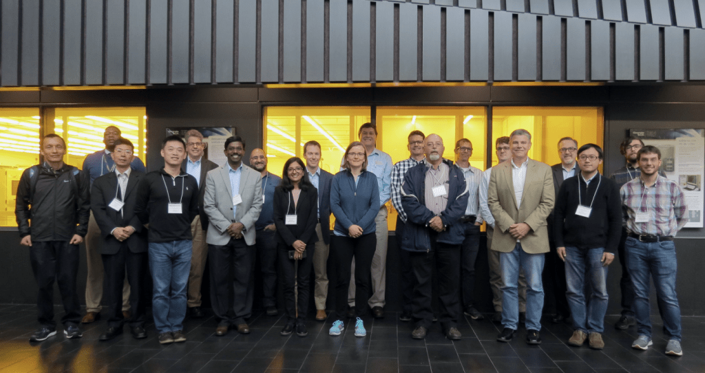
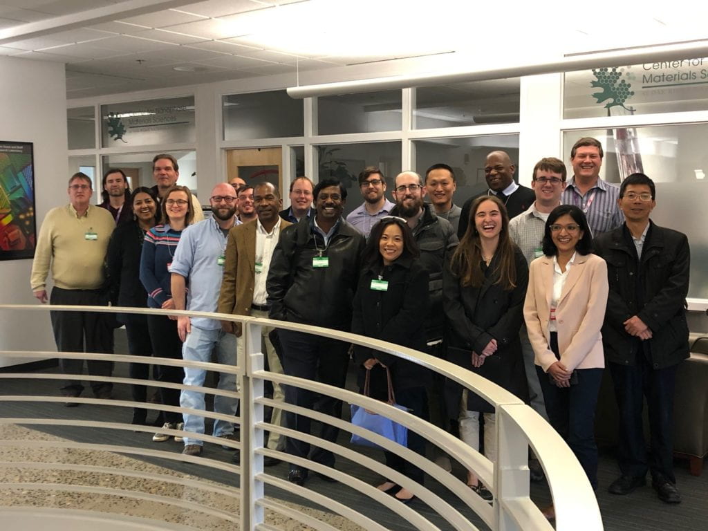
The Southeastern Nano Facility Network (SENFN) was created in 2018 as a regional network of nanoscale science and engineering user facilities located in the SE United States. SENFN had its inaugural meeting on November 12, 2018 at Georgia Tech and a second meeting in 2019 at ORNL. A virtual meeting, discussing the challenges of COVID-19, took place in 2020.

Inaugural Meeting of SENFN at Georgia Tech (2018)
SENFN Meeting at ORNL (2019)

The objectives of this network are to share information on capabilities and events at each facility, discuss best-practice solutions to common challenges, and begin a process for informal staff-level technical exchanges. SENFN includes the institutions listed below. If you are interested in joining SENFN, please contact Dr. David Gottfried.

University Facility
Alabama A&M University Electrical Engineering Laboratories
Clemson University Micro Fabrication Facility
Duke University Shared Materials Instrumentation Facility (SMIF)
Florida International University Advanced Materials Engineering Research Institute
Georgia Institute of Technology Micro/Nano Fabrication Facility
Materials Characterization Facility (MCF)
Georgia Southern University Small Scale Fabrication and Characterization (SSFC) Labs
Joint School of Nanoscience and Nanoengineering JSNN Facilities
Louisiana State University Center for Advanced Microstructures and Devices
NC State University NCSU Nanofabrication Facility
Analytical Instrumentation Facility (AIF)
Oak Ridge National Lab Center for Nanophase Materials Science
Tulane University Micro/Nano Fabrication Facility
University of Alabama Micro-Fabrication Facility
University of Alabama-Huntsville Nano and Micro Devices Center
University of Florida Research Service Centers
University of Georgia Integrated Bioscience and Nanotechnology Cleanroom
University of Memphis Integrated Microscopy Center
University of North Carolina-Chapel Hill Chapel Hill Analytical and Nanofabrication Laboratory (CHANL)
University of Central Florida Nanoscience Technology Center
University of South Carolina Micro/Nanofluidics Lab
University of South Florida Nanotechnology Research and Education Center (NREC)
University of Tennessee-Knoxville Joint Institute for Advanced Materials Micro-Processing Research Facility
Vanderbilt University Vanderbilt Institute of Nanoscale Science & Engineering (VINSE)

While all SENFN facilities include tools and expertise for nanoscale fabrication and characterization, some of these facilities contain unique capabilities that are available to the broader scientific community.

Clemson COMSET operates an Optical Fiber Laboratory, which is the only academic facility in the United States with industry-grade capabilities for fabricating optical fiber. The Optical Fiber Laboratory comprises an SG Controls MCVD lathe and Heathway Fiber Draw Tower along with a preform and fiber characterization laboratory as well as a staff of three on-site researchers with more than 40 years of cumulative industrial experience in the optical fiber industry.

JSNN includes the Gateway Materials Test Center (GMTC) which can perform composite and textile testing. Also located within the JSNN Microscopy Lab is a Zeiss Orion Plus Helium Ion Microscope.

UNC CHANL facility includes capability for hot embossing a mold into a thermoplastic material at temperatures above its glass transition temperature with an applied force. This tool allows temperatures up to 320º, pressures up to 20 tons, front and backside embossing with alignment, with capabilities of embossing features on the micron and nanoscale.

ORNL Microwave Plasma Enhanced Nano-Crystaline Diamond Deposition

Biocleanrooms are located at several of the institutions, including Georgia Tech, JSNN, and University of Georgia

News and Events

  • Spring 2025 Microfabrication Short Course Registration is Now OPEN! February 26, 2025
  • Summer 2025 Internship Program – Applications Now Accepted December 5, 2024
  • Summer 2024 Internship Program – Applications Now Accepted December 13, 2023
  • Fall 2023 Nano@Tech Seminars August 30, 2023
  • SENIC June 2023 Newsletter June 1, 2023

Social Media Links

  • Facebook
  • LinkedIn
  • Twitter

Copyright © 2025 · Education Pro on Genesis Framework · WordPress · Log in